
Larry East, W1HUE
Tucson, Arizona
(contact author)
The original version of this article was published in the April, 2000
issue of the ARCI QRP Quarterly
The NorCal 20 QRP 20m transceiver was sold as a limited edition kit by the Northern California QRP Club (NorCal) in early 1999. It was later sold as a commercial kit by "Red Hot Radio", a small company started by Dave Fifield, AD6A (the NorCal 20's designer). It is a well designed little rig, but even the best can sometimes use a little "tweaking". Some modifications that I found useful are described in this note. They are:
Some NC20's have a noticeable keying chirp (or "whoop", as some have called it) on transmit. This is caused by the +12V supply voltage "sagging" slightly from the increased transmit current drain. A 78L08 linear regulator provides the reference voltage for the VCO (voltage controlled VFO) and any change in its output voltage will produce a change in the VCO frequency. 78Lxx regulators do not have perfect line regulation, and a few tenths of a volt change in input voltage can cause a few millivolts change in output voltage. An instantaneous change would not be noticed when the transmitter is keyed. However, the +12V supply voltage does not change instantaneously when the transmitter is keyed. In addition, there is a time constant associated with the reference voltage on pin 3 of U1. The net result is that it takes a fraction of a second for the VFO frequency to shift (a few tens of Hz, typically) and this is manifested as a "chirp" in the transmitted signal.
There are two recommended cures for this problem:
Applying one or both of these "fixes" seems to work in most cases.
However, I decided to go to the heart of the problem and provide a very stable VCO reference voltage by using "double regulation". I did this by placing a 9V regulator IC ahead of the 78L08 to isolate it as much as possible from any change in the +12V supply buss. Since the input to the 78L08 needs to be at least 2V higher than its output for proper regulation, I increased the 9V regulator's output to 10.2V by placing two Si diodes between its common lead and ground. (Why not use a 10V regulator? Because I couldn't find one!) The 9V regulator I used is a Toko TK11690; this is a low-dropout type that will maintain regulation as long as its input is greater than ~0.1V above its output. A 79L09 could be used, but the supply voltage would need to be kept above ~12.5V (taking into account the ~0.3V drop across the reverse-polarity protection diode). The TK11690, on the other hand, will maintain regulation with a supply voltage of only 10.6V. I used the TO92 version of the Toko device (same pinout as the 78Lxx devices). However, this is an "obsolete" item and has been replaced by a SOT-89 surface mount version, the TK11690U. Digi-Key currently has the TO-92 version in stock (part no. TK11690CT-ND), but they will not have any more once current inventory is depleted. They also stock the SM version (part no. TK11690UCT-ND); this can be used in the NC20 – but you will need a good pair of tweezers, small soldering iron tip, a steady hand and possibly a magnifying glass!
The dual regulator circuit is shown in the figure below:
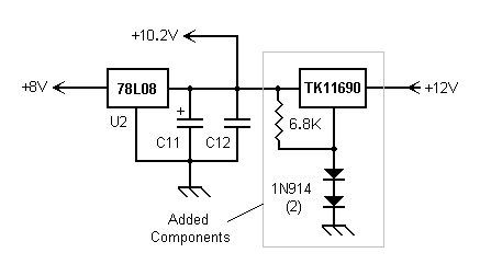
OK, so where did I stick the extra regulator? If you look at the top of the NC20 PC board, you will see a short "jumper trace" starting near C11 and running toward C63. If you follow this trace through to the bottom of the board, you will see that it is part of the +12V supply line to U2. I simply cut that PC trace and "bridged" it with the TK11690. The two 1N914 (or 1N4148) diodes run between the TK's center terminal and the ground pad for C99. The 6.8K resistor (used to insure sufficient current through the diodes) is connected between the TK11690's output and the diodes. Space is a little tight, but it will fit if mounted vertically. Simple, eh?
It is possible to mount the SOT-89 version of the regulator in a similar manner. Make sure that the large single ground tab does not touch anything (it is connected to "common") and the "common" tab is over the break in the PC trace. A good set of tweezers and a small soldering iron tip are definitely needed here!
Before I made this mod, I measured a VFO shift of about 30Hz when the supply voltage was changed 0.5V. This was with the "stock" 78L08. After the mode, a 0.5V change in the supply voltage did not cause any detectable shift (less than 1Hz) in the VFO frequency. Varying the supply voltage from 10.5V to 14V produced a shift of less than 5Hz.
The no-signal AGC voltage is derived from the +12V buss via a voltage divider. It will therefore track any change in the supply voltage. This is not a problem if the supply voltage is relatively stable. However, it could become a problem if multiple power sources are used and not all supply the same voltage. If the AGC no-signal voltage is set when using a "normal voltage" power source and then a lower voltage supply is used, a noticeable drop in receiver gain can occur. Conversely, if a higher supply voltage is used, the AGC may not respond until input signals become rather large.
It would therefore seem advisable to supply the AGC amplifier (Q10 - Q13) with a regulated supply voltage. Some experimenting showed that a supply voltage of at least 9V is needed for the AGC amplifier to function properly. The 10.2V output of the "pre-regulator" described above is therefore just about right! It is a simple matter to use that to power the AGC amp.
To make the mod, proceed as follows:
Locate the PC trace that supplies +12V to the AGC amp. Looking at the bottom of the board with the tuning pot to your right, this trace is just to the right of Q13. Cut this trace between the point where R65 attaches and where it passes through the board. Solder a jumper wire between this trace (the solder pad for R68 or R61 is a convenient attachment point) and the output of the TK11609 (the solder pad for C12 is a convenient attachment point).
That's it! All that remains to be done is readjust VR5 as per instructions in the NC20 manual (or as described in Dave Fifield's AGC mod, which I highly recommend – see comments under Miscellaneous below).
The warmup drift in the AGC zero-signal voltage can be essentially eliminated by a very simple mod: Insert a 1N914 (or 1N4148) in series with R63 to ground (the diode's cathode goes to ground). You can install the diode on top of the board (vertically) next to R63 – cut the lead from R63 to ground and insert the diode. Readjust VR5 for the proper zero-signal AGC voltage; if you can't get the AGC voltage high enough, replace R63 with a smaller value (680 Ohms worked for me). Before I made this mod, the AGC voltage drifted about 300mV during warmup. After the mod, the drift was less than 10mV.
Steve Weber, KD1JV, recently pointed out in a QRP-L post that the best way to obtain sidetone "volume control independence" is to use the second audio input of the LM386 - LM380 audio IC's commonly used in QRP rigs. Since the second input of the NC20's LM380 (pin 2) is connected directly to the ground-plane on top of the board, this would require some effort – especially after the LM380 is installed. I used a simpler, although less elegant, method to isolate the TiCK and AFA outputs from the audio gain control.
This modification will allow the TiCK and AFA audio output levels to be as independent of the audio gain control (VR4) setting as you wish. This mod requires two PCB traces to be cut and one resistor to be added. The resistor value controls the degree to which the TiCK/AFA tones are independent of the audio gain control (VR4) setting. Select the value as follows:
If you want the TiCK and AFA audio levels to be somewhat dependent on the setting of VR4, use a resistor in the range 1-3K (e.g., 2.2K). This is useful if you frequently switch between headphones and a speaker.
If you want the TiCK and AFA tone levels to be essentially independent of the setting of VR4, use a value in the range 5-10K (6.2K works for me. I don't recommend using a value greater than 10K.)
To make the mod, proceed as follows:
That's it! All that remains to be done is to readjust VR7 and VR8 for proper levels of the TiCK and AFA tones, respectively.
I performed the AGC mod described by Dave Fifield (the NorCal 20 designer) and highly recommend it. It makes the AGC operation much smoother. I did not encounter any of the difficulties with "pops" or "screeches" when the rig is keyed reported by some folks on QRP-L. Maybe I'm just lucky. However, the mute circuit must be operating properly; the voltage on pins 1 and 2 of U4 should be reduced to almost zero (certainly below 0.5V) during transmit to eliminate any "bleed through" of transmitter RF into succeeding receiver stages. If it is not, check D17 and D18. Diodes D5-D8 must also be connected correctly to protect the receiver input from RF.
I replaced Q1 and Q5 with 2N5457's as recommended by Dave Fifield. However, I still had a problem with Q1 not turning off during transmit when the RIT pot was near the ground end. Using a J309 solved the problem, but a different 2N5457 would probably have also worked (there is considerable variation in the gate cutoff voltage between FETs of the same type). You can make a simple test to see if Q1 is being turned off during transmit: Listen to the output of the transmitter on another receiver and rotate the RIT control. If the transmit frequency varies with the RIT pot setting, then Q1 is not being turned off completely; replace it with another 2N5457 (or J309) and test again.
Something else I did was replace Q6 with a 2N5109 because I believe it to be a lower noise device than a 2N4127. I did not make and before/after noise or sensitivity comparisons (I installed the 2N5109 as I was building the kit), so I don't know if it made any real difference. I also substituted an MRF904 for Q7; again, no before/after comparisons were made. However, the receiver is very sensitive and I can hear anything that I can hear on other rigs (and then some), so it does not appear that these substitutions did any harm!
Note added March, 2002
Later, I checked the MDS (minimum detectable signal) of my NC20 with a calibrated signal generator and wideband AC Voltmeter. After peaking all of the receiver's tuned circuits, I measured an MDS of -134dBm – provided that the audio gain control was at least 40% or so of maximum. With the audio gain at about 20% of maximum, the MDS dropped to -128dBm. Others have reported MDS values of -130dBm or better for stock NC20's – so the transistor substitutions probably made little if any improvement.
————
Copyright © 2005, 2017 by Larry East, W1HUE ————
Page last updated on July 6, 2017