
Larry East, W1HUE
Tucson, Arizona
(contact author)
Reprinted from the April 1997 ARCI QRP Quarterly
Before making any mods described in this article, be sure to read the Notes and Corrections article.
This is the second of a two-part series describing modifications that I have made to my Index Laboratories QRP PLUS transceiver. Part 1 appeared in the January 1997 issue of The QRP Quarterly and dealt with modifications that are primarily receiver related. In this second part, I will describe modifications that I have made to improve the transmitter performance. Many of the modifications are specific to the "original" version of the transceiver, but some are also applicable to the "new improved" version that became available in the spring of 1996. From this point on, I will use "QRP+" when referring specifically to the original model and "QRP++" when referring to the new model (including old models that have been updated by the factory). I will use "QRP PLUS" in non-model specific references.
I will also give some advice on final amplifier bias adjustment for those not wishing to modify the final amplifier.
I presented several things in Part 1 that should be kept in mind when working on a QRP PLUS. I also gave information on obtaining the latest firmware upgrade from the factory. If you do not have a copy of that article, I will be glad to provide one if you send me a business size SASE. One item is worth repeating, however: If you remove the AF board (the one with the 3V memory backup battery), make sure to hold down the MEM button when you apply power to the rig after reassembly (if you forget, just do it the next time you apply power).
Please keep in mind the need for carefully soldering and cleanliness when working on these rather compact boards. It's very easy to bridge a couple of traces with solder or a piece of a component lead. Also check for and remove the metal shavings that tend to accumulate around the board mounting holes from wear and tear produced by removing and replacing the boards.
Some additional observations that I have made regarding receiver microphonics might be of interest. I stated in Part 1 that the microphonics could be reduced by using larger foam rubber pads above and below the LO board. Now I’m not so sure that really helps much. It appears that keeping the board hold-down bolts good and tight is the critical factor in keeping microphonics under control. In fact, I inadvertently left the foam pads out one time that I reassembled my rig, and the microphonics appeared to be less than with the pads installed!
The following modifications are described in this article:
Since the QRP PLUS has a "full coverage" receiver, it is difficult to incorporate band-pass filters (particularly in such a small radio) in the design to insure the elimination of unwanted transmitter output signals (spurious signals or simply "spurs"). Spurs can arise from higher order mixing products between the local oscillator and its harmonics and other signals present and their harmonics. Such mixing products can be accentuated or even produced by any nonlinearity in the transmitter amplifying chain.
The QRP-PLUS uses relatively high local oscillator frequencies and a 50MHz IF in an attempt to keep any spurs above the carrier frequency so that they can be removed by simple low pass filters. However, there are a few spurs that occur below the carrier frequency when operating on 14Mhz and above, and a few very close to the operating frequency, particularly on 12M. The majority of these spurs are more than 30dB below the carrier level and therefore are of no great concern. However, the QRP+ is plagued with some spurs several MHz below the carrier that are not much more than 20dB down when operating on 15M and 10M. The presence of these spurs also causes the transmitter output to appear rather "ragged" when viewed on an oscilloscope. I was able to make some spectrum measurements on one QRP++ and those spurs were at least 30dB down. The improvement in the QRP++ is evidently due to an improved IF amplifier design and/or a different mixer. Both models of the QRP PLUS are plagued by close-in spurs on 12M that may be less than 30dB down. More on this later.
Some relatively simple modifications can be made to the QRP+ to reduce the below-the-carrier spurs. All of these mods are made to the RF board which is the top one in the stack.
Note: The spur reduction modifications described below are specific to the QRP+.
The first and most complex mod makes the transmitter IF amplifier stage that follows the crystal filter resonant at 50MHz. One would think that this should be unnecessary, but apparently some lower frequencies are being passed by the overtone crystals in the filter. This modification has been posted on the Internet several times and I’m not sure who originally came up with the idea, but it wasn’t me. To perform this mod, proceed as follows:
When this mod is completed, the resulting circuit should be as shown in Figure 1. The replacement for L11 must be pretty close to 50nH; otherwise transmitter power will suffer. If it is really far off the mark, you will get no output at all! I first attempted to use a small toroid (T16-10) with a few turns but I had trouble getting it to resonate at exactly 50MHz. I then tried two 100nH chokes in parallel and that worked just fine. I suspect that the chokes have a lower Q than the toroid and produce a broader resonant peak.
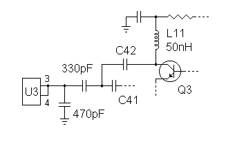
Figure 1. Modified IF filter buffer amplifier.
I found that this modification produced a significant reduction in most of the spurs, but there were still a couple within 30 dB of the carrier level when operating on 15M and 10M. In addition, the 20M, 15M and 10M transmitter output still appeared a bit "ragged" on my ‘scope. One very simple change to the low pass filter following the mixer solved the problem: I added a 20pF capacitor across L7 (on the bottom of the board). The cap forms a parallel resonant circuit with L7 at approximately 50MHz, sharply reducing IF feedthrough. It also sharpens the high frequency roll-off of the LP filter resulting in greater attenuation for all frequencies above about 30 MHz. After this simple change, the transmitter output looked much better on the ‘scope and all spurs (except the ones unique to 12M) were at least 35dB down. Before adding the capacitor across L7, you should check the transmitter output at the high end of 10M, say 29MHz, relative to the output at 28MHz. If the output at 29MHz is reduced significantly (more than 0.25W or so) after adding 20pF across L7, try a smaller cap (but not less than 10pF).
Adding one more capacitor—56pF from the junction of L4 and C17 (the output of Q10) to ground—finally brought all the below-the-carrier spurs down to at least the 40 dBc level; some spurs originally seen are no longer measurable. Adding this capacitor also made the 20M and above output from Q10 look much better on the ‘scope. The exact size of this cap is not especially critical; anything from 47pF to 100pF seems to do the job. However, values above about 68pF resulted in less transmitter output above 20M, so I settled on a value of 56pF.
As noted above, 12M has a special problem: Higher order mixing products result in spurs very close to the carrier frequency. These spurs are related to the carrier frequency, F0, the 50MHz IF and LO (local oscillator) frequencies as follows:
F0 ± N x (2 x IF – (LO + F0 ))
where N is a positive integer (1, 2, 3, ...). This can be rearranged to better show the mixing products between the carrier injection (IF) and local oscillator (LO) frequencies:
(3N – 1) x IF – (2N – 1) x LO
and
(2N + 1) x LO – (3N + 1) x IF
For example, at a carrier frequency of 24.9 MHz, mixing products cause spurs at ±200 kHz, ±400 kHz, etc. from the carrier frequency, decreasing in amplitude with increasing values of N. In my unmodified QRP+, the "first order" (N = 1) mixing products were rather strong; only 28dB down from a 5W carrier frequency of 24.90MHz and 22dB down at 24.95MHz. Reducing the output power to 2W reduced these spurs to 40 dBc and 32 dBc respectively. These spurs were somewhat lower on the one QRP++ that I have tested, but still not below the 30 dBc level when operating in the top 40 kHz or so of the band at a power output of 5W.
What can be done to reduce these spurs? Well, I tried everything I could think of without any noticeable improvement — until I replaced the final amplifier as described later. A good part of the problem appears to be caused by the non-linear operation of the stock IRF510 MOSFET final amplifier at output powers greater than 2 or 3 Watts. With the new final amplifier, the 12M spurs are at least 30 dBc at 5W output except at the very top edge of the band where they are about 28 dBc — still not entirely ‘legal’ but a good 15 dB improvement.
If you don’t do the final amplifier modification described later, you can take the following steps to keep the 12M spurs down to a reasonable level: 1) Make sure that the bias on the final amplifier is properly adjusted (discussed later). 2) Keep the output power no higher than 3W. 3) Avoid operating in the top 40kHz or so of the band.
The QRP PLUS (both the "+" and "++" versions) uses individual five-pole "elliptic" low pass filters in the transmitter output on 160M, 80M and 40M. Above 40M, five-pole Chebyshev filters are used, and a single filter is used for two adjacent bands. That is, one filter is used for 30M and 20M, another one for 17M and 15M, and a third for 12M and 10M. It is interesting that elliptic filters are used on the lowest three bands but not on the higher bands where the sharper high frequency roll-off of such filters are really needed. The second harmonic output on 160M through 40M is at least 50dB below the carrier level, whereas it ranges from slightly more than 30 dBc for 30M to about 50 dBc for 20M and 10M. Higher harmonics are at least 50 dBc on all bands.
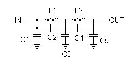
Figure 2. Five-pole elliptic low pass filter.
Changing the three high-band filters to elliptic filter designs reduced the second harmonic levels to at least 45dBc. I also obtained greater output power with the new filters, ranging from an increase of almost 3W on 30M to about 0.5W on 10M. Figure 2 shows a schematic of a five-pole elliptic filter. The component values for each filter are given in Table 1.
Table 1. New high-band LP filter component values (see Figure 2).
| Component | 30/20M | 17/15M | 12/10M |
|---|---|---|---|
| L1 |
610 nH 11T on T50-6 |
400 nH 9T on T50-6 |
320 nH 10T on T50-10 |
| L2 |
380 nH 9T on T50-6 |
320 nH 10T on T50-10 |
220 nH 8T on T50-10 |
| C1 | 150 pF | 82 pF | 62 pF |
| C2 | 47 pF | 20 pF | 15 pF |
| C3 | 270 pF | 180 pF | (120 + 20) pF |
| C4 | (150 + 10) pF | 68 pF | 47 pF |
| C5 | 82 pF | 56 pF | 39 pF |
I used 300V silver mica capacitors in the new filters, but good quality
NPO (or C0G) ceramic caps rated for at least 100V should work just as
well. The capacitors across the coils must be mounted on the bottom
(trace side) of the PC board. I also mounted the smaller of the two
paralleled capacitors used in the 30/20M and 12/10M filters on the bottom
of the board. (Two capacitance values shown in Table 1 separated by a "+"
indicates that two capacitors are to be used in parallel.)
I used number 22 enameled wire to wind the inductors; you can simply remove the required number of turns from the original coils where T50-6 cores are used. Remember that each time a wire passes through the center hole of a toroid it counts as one turn. I found that T50-10 cores were better to use for the lower inductance value. The fewer turns required using the original T50-6 cores made them too sensitive to tightness and spacing of the windings. Note that L1 for the 17/15M filter and L2 for the 30/20M filter have the same number of turns but slightly different inductance values; the turns on the 17/15M coil are more closely spaced than the 30/20M coil. It would be a good idea to measure the inductance values of the finished coils, if you have some way of doing that.
The values of the input capacitors for the three low-band filters can be reduced slightly to improve the response flatness of these filters at the high end of their passbands. I changed the input cap for the 80M filter (C6 on the "XMTR" board schematic) from 820pF to 750pF and the 40M filter input cap (C11) from 390pF to 360pF. The 160M input filter cap should be about 1400pF; the 1500pF value is certainly close enough. These changes result in less attenuation imposed by the output filters at the high ends of 75M and 40M without making any measurable differences in their harmonic attenuation.
"Before" and "after" comparisons of the second and third harmonic intensities at 5W output are shown in Table 2. The harmonic intensities were determined using a borrowed IFR-1500 spectrum analyzer that had a dynamic range of about 60dB at the 5W level. The only band that did not show an improvement was 20M, which was the only high-band for which the second harmonic was less than 50dBc with the stock filter. The biggest improvements were for 30M and 12M; the new filters provide a 15dB or so reduction in the second harmonics on these bands. Your results may vary somewhat due to normal component value tolerances.
You might well ask: "Is it worth the effort to replace these filters?" The answer to that depends on whether or not you need — either from a legal or personal preference standpoint — to keep harmonic levels at least 40dB down. If you can live with >30dB, then don’t bother. On the other hand, it really isn’t that much effort to change them.
Table 2. Harmonic levels obtained with original and modified filters.
| Carrier | Harmonic Content – dB Below Carrier | |||
| Freq., F0 | Original Output Filters | New Output Filters | ||
| (MHz) | 2 x F0 | 3 x F0 | 2 x F0 | 3 x F0 |
| 1.820 | 50 | >60 | - - - | - - - |
| 3.560 | 55 | >60 | - - - | - - - |
| 7.040 | 52 | >60 | - - - | - - - |
| 10.116 | 34 | 53 | 49 | >60 |
| 14.060 | 52 | >60 | 52 | >60 |
| 18.070 | 40 | ~60 | 50 | >60 |
| 21.060 | 37 | ~60 | 45 | ~60 |
| 24.900 | 36 | 54 | 52 | >60 |
| 28.060 | 48 | 58 | 52 | 58 |
The Rev 4C EPROM for the QRP+ contains firmware code changes that eliminate the "forced spacing" characteristic of the internal keyer which many users (myself included) found rather annoying. The Rev 4C keyer firmware changes also allow an external keyer to be used at speeds up to about 40 wpm whereas the Rev 03 and earlier EPROMs would not allow external keying above 25 to 30 wpm. The bandpass characteristics of the SCAF at bandwidth settings of 1.0 kHz and below are also changed by this EPROM to better center the passband around the 800 Hz CW offset frequency. These changes essentially make the keying and SCAF filter passbands the same as the QRP++.
A disappointing side-effect of the Rev 4C code is that keying is very mushy when in normal XCEVE mode; the rise time of the transmitter output envelope is almost 10ms! When the front panel mode switch is in the RIT or SPLIT position, the keyed output risetime is about 2ms — the same as with the Rev 03 code — resulting in much better sounding keying. "What’s going on here," you may well ask (as did I). To answer that requires a little explanation of the keying sequence in the rig. When the rig is keyed, +12V is immediately applied to the transmitter driver stages and the antenna is switched from the receive to the transmit RF chain. However, the actual keying signal (a voltage applied to the balanced modulator to unbalance it and let RF pass) is delayed slightly — about 5ms in XCEVE and about 25 ms if RIT or SPLIT is turned on. This delay was much longer with previous firmware versions, resulting in the limited external keying speed. The 5ms delay when in XCEVE does not allow the bias on the first driver transistor to reach its final operating point resulting in the slow rise of the output RF envelope. Does this mean that one must leave the mode switch in RIT or SPLIT to get decent keying? Not if you are willing to make a simple modification to the RF board: simply decrease the size of C54 by a factor of ten — from 4.7µF to 0.47µF (use a dipped tantalum cap). This change will result in a 2ms risetime when in XCEVE as well as RIT and SPLIT modes. The RF board is the top one in the stack, and C54 is located in the rear left-hand quadrant of the board (when viewed from the front of the rig).
Another keying related problem can also occur with the Rev 4C EPROM: an RIT or SPLIT receive/transmit offset of more than 3 to 5 kHz (depending on the band) can result in a noticeable "chirp" on the keyed signal. The chirp became very pronounced in my rig at offsets of 10kHz or more. With the Rev 03 EPROM installed, I could not detect any noticeable chip below a receive/transmit offset of 15 to 20 kHz (depending on the band). The Rev 4C EPROM provides less delay between key-down and transmitter output in order to accommodate faster external keying (see above), but this reduced delay does not give the PLL sufficient time to stabilize the VCO frequency. I have seen complaints from others about chirp with this EPROM even with no RIT offset, so the PLL settling time may vary somewhat from rig to rig.
However, the chirp can be cured — at least for receive/transmit offsets that are not too great — by replacing a couple of caps on the LO board. Changing C43 and C44 from 4.7µF (original values) to 2.2 µF in my rig resulted in no detectable chirp for receive/transmit offsets up to at least 20 kHz. This is good enough for "DX split" operation, which is typically no more than 10 kHz on CW. Some care is in order when fiddling with these cap values; reducing the values too much can result in the PLL becoming unstable. I did not try to determine the smallest values that can be safely used since 2.2µF seemed to do the trick. C43 and C44 are located near the LO board’s righthand rear edge (when viewed from the front of the rig).
The microprocessor in the QRP+ can be "locked up" by rapidly opening and closing the push-to-talk switch on the microphone, or by a "bouncy" PTT switch. As far as I know, this problem does not occur in the QRP++ due to changes in the PTT circuitry. Several suggestions have been posted to the Internet QRP discussion group on ways to reduce this problem, including installing a bypass capacitor across the PTT switch and an isolation diode in the PTT line. I did both and found a considerable improvement. A really bad PTT switch can still cause problems, however. I also installed an isolation diode in series with the straight key input just in case any "funny stuff" might happen to be introduced by an external keyer. These modifications are depicted in Figure 3. I added the bypass caps directly from the J4 and J6 jack connections to ground on the bottom of the "AF" PC board. Rather than try to explain which jack connections should be bypassed, I suggest that you use a "naked" plug and Ohm meter and trace the connections yourself; that way I won’t get blamed if you do it wrong!
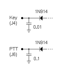
Figure 3. Key and PTT line noise immunity mods.
It is necessary to cut a couple of traces on the PC board in order to install the isolation diodes. I installed the diode in the key line by cutting the trace from the key jack (use an Ohm meter to make sure you have the right one) that passes just to the right of the backup battery (as viewed from the front of the board). I cut the trace just to the left of R8 and "tack-soldered" the diode to the trace on each side of the cut. Use a sharp "hobby knife" or razor blade to cut the trace. Be careful; there’s not much room for mistakes here! A convenient point to install the diode in the PTT line is between C45 and R17. Again, use an Ohm meter to make sure you have the right trace.
The IRF510 "HEXFET®" that is used in the QRP PLUS final amplifier was designed for use in voltage switching applications rather than as an RF amplifier. However, this type of power FET works quite well as a class C or D RF amplifiers at HF frequencies. (Power FETs designed especially for RF work can be used well into the VHF range, but they are rather expensive.) However, it appears that the IRF510 does not function well as a linear amplifier when its drain voltage is less than 20V or so. I discovered this when I attempted to modify the ALC circuit to obtain more SSB power. When I ran some "two-tone" tests and viewed the SSB output on an oscilloscope, I discovered that "flattopping" occurred at output power levels greater than about 3W. This was on 75M; flattopping occurred at about 1.5W on 10M! Looking at the output of the driver (isolated from the final and terminated in 50 Ohms) showed no indications of flattopping at a level sufficient to produce an output from the final in excess of 7W on CW. This indicated that the limited linear operating range was due to a problem in the final amplifier. My initial tests were made with a supply voltage of 13.2V. Increasing the voltage to 14V improved the situation somewhat: Flattopping then did not occur until just under 4W output on 75M.
I then decided to check the final amplifier bias and, in the process, discovered an error (two, actually) in my manual. The instructions for setting the transmitter output stage bias states that minimum current will occur with the bias control set fully counter clockwise; in fact, minimum current occurs with the control fully clockwise. It goes on to state that the bias control should be adjusted to produce an increase in transmitter idling current of 60mA. This is also incorrect: an increase of at least 400mA is required to achieve decent linear operation from the final. The first error has been corrected in later versions of the manual. The second error has been almost corrected: The instructions now say to set the total idling current to 600mA, whereas I found that a value of at least 850mA is required (at a supply voltage of 13.2V) for linear operation. Setting the bias as instructed in my manual (for an increase of 60mA) resulted in severe "crossover" distortion in SSB mode. (It also resulted in stronger 12M spurs, by the way.) If you set the final bias following the incorrect manual instructions, by all means reset it!
My observations concerning the limited linear operating range and the high idling current required were confirmed by Internet conversations with Peter Zenker, DL2FI, of the Berlin QRP Club. Peter stated that current measurements made on several "factory fresh" rigs showed transmitter idling currents in the range 800mA to 1200mA. He also confirmed that no more than about 3W of undistorted SSB power can be obtained when operating from "12V power sources" (which typically deliver between 13V and 13.5V). He also stated that some members of the Berlin club were using 24V to power the IRF510 final amplifier and obtaining "perfect SSB at 5W or more output."
Note:
Power sources delivering more than 15V should not be used to power
the entire rig. Doing so will exceed the maximum voltage
ratings on some components!
Before leaving the subject of final amplifier bias, there is something that you should check in your rig if you have one of the early models: Make sure that a 78L05 is used to supply a regulated bias voltage for the IRF510. Early production models used a simple voltage divider from the +12V bus, and that arrangement is still shown in the schematic in the manual. Look at the RF board just in front of the bias control; there should be what looks like a transistor in the spot marked "R14". This is a 78L05 voltage regulator. If there is a resistor there instead, you should definitely make the following modification:
Before considering this mod, READ THIS.
After discovering the linearity problem with the IRF510, I decided to see if I could find a replacement device that would work better at 12V. An Internet inquiry brought responses from Dana Myers, K6JQ, and Jim Kortge, K8IQY, suggesting that I try a Motorola MTP3055E "TMOS®" power FET. Both had good experience using this device as a tuned RF amplifier, but neither had tried using one as a broad band amplifier. Dana, in true ham tradition, even offered to send me a couple to experiment with! The MTP3055E has the same physical configuration and printouts as the IRF510 so it was an easy matter to simply replace the original final and see what happened. Not only did it work, but some quick measurements indicated that it could produce an undistorted SSB output of at least 5 Watts and at a lower idling current than required by the IRF510! However, the power consumption for a given output power was greater than with the IRF510, particularly on 10M. In addition, the output power dropped rather severely above 20M; I could get in excess of 10W out on 160M and 80M but barely 5W on 10M. After some discussions with Dana, I replaced the stock 4:1 impedance ratio output transformer with one having a 16:1 impedance ratio. What a difference that made: I could get almost 10W out on 10M!
I won’t bore you with the details of all the experimenting that I did; I’ll just give you my final results. The revised final amplifier circuit shown in Figure 4 is capable of producing a 6W to 7W undistorted SSB output into 50 Ohms on all bands from 160M through 10M when operated from a supply voltage of 13.2V. Linearity remains good at 5W on the lower bands and 4W on 10M even when operated from 12.0V. Ah, sweet smell of success! (Much better than the smell of fried capacitors, by the way...)
The new output transformer that I finally settled on is wound on an Amidon 61-202 binocular (two hole) core and has a two turn primary and five turn secondary. This gives an impedance ratio of about 12:1. The large ratio is required to "swamp" the very high dynamic output capacitance of the MTP3055E — according to Dana, this is about 2.5 times the "static" output capacitance of 300pF, or approximately 750pF! I used #22 enameled wire for the primary and #26 for the secondary, although #24 could be used for both (anything larger won’t allow enough turns through the core).
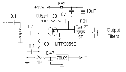
Figure 4. Modified transmitter output amplifier.
To make the new output transformer, start with a five inch length of #22 (or #24) wire and a 12 inch length of #26 (or #24). Align one end of each of the two wires and twist them together to produce between four and six twists per inch. I suggest doing this by hand with the aligned ends of the wires clamped in a vice. Place the twisted end of the wires through one hole of the core, allowing it to extend about 3/4 inch from the other end. Then feed the other (long) end of the wires through the other whole. This constitutes one turn. Feed the long end of the wires through the two holes again; you have now completed the two turn primary and two turns of the secondary. Untwist the wires that extend from the core; you should now have four wires extending from the same end of the core, two from each hole. Pass the long wire (the #26 wire) through each hole of the core three more times to complete the secondary. You should again have four wires extending from one end of the core, two from each hole. Trim the ends of the wires to about 3/4 inch, remove the enamel and tin them. Twist one of the primary wires together with the opposite secondary wire; that is, the secondary wire sticking out of the opposite hole. These twisted leads will connect to the MTP3055E drain when the transformer is installed.
The gate to source feedback network consisting of 600nH in series with 33 Ohms flattens the response of the amplifier (the 0.1uF capacitor is used for DC blocking and has little effect above 80M). For a given setting of the CW drive control, the power output of my rig (the QRP+ has no ALC in CW mode) with the new final remains constant within a factor of two from 1.8MHz to 29.7MHz. Without the feedback network, output power dropped by a factor of about six over this range (the output from the original IRF510 final dropped by about a factor of four). I have no theoretical basis for the L, C and R values used in the feedback network; I simply experimented until I got something that seemed to work! The feedback network is undoubtedly not optimum, but the performance is certainly acceptable. Besides, there are other factors in additional to the final amplifier that affect changes in power output with frequency. I made the 600nH inductor by winding 12 turns of #26 wire on an Amidon T30-2 core. Wire size is not critical; anything from #28 to #24 can be used. The core type is also not critical; 13 turns on a T30-6 core should also work.
FB1 and FB2 are RF chokes made from Amidon FB101-64 ferrite beads. FB1 slips over the "cold" output transformer lead; its function is to "de-Q" the output transformer for better stability. FB2 consists of a piece of #24 wire passed twice through a bead and was "tack soldered" across a gap cut in the 12V bus between C28 (the 10uF molded tantalum capacitor) and Q8 (the driver transistor). Its function is to provide additional isolation between the driver stage and the final.
Now that we have the preliminaries taken care of, I’ll outline the steps to follow if you feel up to making this modification. Please note, however, that I have only performed this mod on one rig — my QRP+. My results are hopefully reproducible, and the new final should work just fine with a QRP++. Unless Mr. Murphy decides to intervene, of course! The parts that you will need to modify the final are as follows:
1 – MTP3055E power FET (available from Newark Electronics).
1 – Amidon 61-202 binocular core.
1 – Amidon T30-2 (or T30-6) toroid core.
2 – Amidon FB101-64 ferrite beads.
2 – 100 Ohm 1/4W composition resistors.
1 – 33 Ohm 1/2W (don’t use 1/4W) composition resistor.
1 – 2.7K 1/4W composition resistor.
1 – 1.5K 1/4W composition resistor (QRP+ only).
1 – 0.1µF monolithic capacitor (small 50V type).
1 – 0.47µF monolithic or dipped tantalum capacitor.
Some #22 and #26 (or #24) enameled wire, solder, etc.
Don’t worry about not seeing a 2.7K, 1.5K or second 100 Ohm resistor in Figure 4; their use will be described later. The 0.47µF capacitor will be used to bypass the output of the 78L05 bias voltage regulator; these things can oscillate if their output is not bypassed and I just don’t trust them! The capacitor size is not critical; anything in the range 0.2µF to 2µF can be used; just make sure it is small enough to fit under the PC board.
Now for the step by step instructions:
Note:
If you have a QRP+ and have installed a resistor from pin 2 of U2 on the AF board to ground in an attempt to get more SSB power, remove it! I have seen this suggested as a way of decreasing the ALC sensitivity, but this actually overrides ALC control.
If everything looks OK, hook up a microphone and check the SSB output with a peak reading Wattmeter or oscilloscope. You should get a good 5W peak output with no "flattopping" or other distortion. If steady tones are fed into the microphone input of a QRP+ (and possibly a QRP++), the ALC will limit the output to between 3W and 4W. However, voice modulation should easily produce a peak output of 5W or more. If you think that the output is a little low on a QRP+, increase the size of R16 on the RF board to 3.3K. (As noted above, shunting the control input of U2 on the AF board to ground with a resistor is not the proper way to control SSB power output!) You should be able to set the peak SSB output power on a QRP++ to 5W or more using the power control. If not, you may have to experiment with different values of R20 on the AF board and/or R16 on the RF board.
The final test is to make some on-the-air SSB contacts, preferably with someone you have talked to before so you can get a before and after comparison. When I ran some tests with a local ham after completing this mod, he told me that I had the best sounding QRP PLUS that he had ever heard!
I believe that this mod is worth doing even if you don’t do much SSB operating. The MTP3055E is a much more rugged device than the IRF510 and therefore more likely to survive such abuses as extremely high SWR (like a shorted antenna lead!). The greater linear operating range also results in a significant reduction of those pesky 12M spurs that I discussed above. The lower transmitter idling current is also something to consider if you do much portable operating, although this really makes little difference when operating CW. The cost of this mode is surprisingly low; the price for a MTP3055E in the Newark catalog is $1.05 — about the same as an IRF510! (But then there’s that blasted $25 order minimum.)
Note: A new version is now available, the MTP3055V. This device will work just as well (possibly better) than the older "E" version. Do not, however, use a "VL" (or "EL") version; this device has a much higher gate capacitance.
See a later article concerning temperature stabilizing the operating point of the MTP3055E (read it here ).
I have used up more that my allotted share of space, I’m afraid. I hope I have presented some information that you have found useful, or at least given you some ideas of things to try — perhaps not only to improve your QRP PLUS but something that you can apply to some of your other projects as well.
You may well wonder why someone would buy a new rig and then spend countless hours trying to make improvements to it. Well, I guess I have gotten a bit carried away with all these modifications and enhancements, but I have found it to be a great learning experience. I have learned how SCAF’s work, how to design low pass filters, some things about broadband FET power amplifiers, and on and on. And I’ve certainly honed my trouble shooting skills when things I tried didn’t work the way I expected! Am I finished trying new things with my QRP+? Probably not; lets see now, I wonder what it would take to make a variable passband IF filter? How about a good IF notch filter? And that AGC system still leaves some things to be desired. Hmmm.... But what about all those unbuilt (and partially built) kits stashed under my work bench? Ah, so many projects and so little time!
My thanks to all with whom I have discussed — in person, over the air and
via the Internet — various aspects of the QRP PLUS and modifications that
I and others have done. Particular thanks go to Peter Zenker, DL2FI, and
Dana Myers, K6JQ. I am also indebted to Niel Skousen, WA7SSA, for the use
of his spectrum analyzer. Last but not least: Thank you, Index
Laboratories, for designing this nice little rig!
Appendix
MTP3055E Reference Data
(From Motorola Technical Data Sheet)
| Max Drain-Source Voltage: | 60V |
| Maximum Drain-Gate Voltage: | 60V |
| Maximum Gate-Source Voltage: | ±20V |
| Maximum Drain Current: | 12A |
| Maximum Power Dissipation: | 40W (at 25 °C) |
| Gate Threshold Voltage: | 2V min, 4.5V max |
| Forward Transconductance: | 4 mhos min |
| Input Capacitance: | 500 pF max |
| Output Capacitance: | 300 pF max |
| Reverse Transfer Capacitance: | 100 pF max |
| Turn-On Delay Time: | 20ns max |
| Rise Time: | 60ns max |
| Turn Off Delay Time: | 65ns max |
| Fall Time: | 65ns max |
———
Copyright © 2005, 2012 by Larry East, W1HUE ———
Page last updated on June 21, 2012