
Larry East, W1HUE
Tucson, Arizona
(contact author)
MFJ Cub transceivers can be easily modified to provide the following:
No circuit board traces need to be cut, but one surface mounted resistor must be removed. Only six additional parts are required:
Note: Mouser part numbers are examples only (and may be out-of-date); equivalent parts from other sources can certainly be used.
It is not absolutely necessary to remove the board from the case, but it probably more convenient to do so (you must, however remove the top cover...). A good magnifying lamp and/or "cheater glasses" will be very helpful; but if you are like me, you needed those to build the kit in the first place!
Start by removing R30. This is a 4.7K SMT resistor located near the right-rear edge of the PC board (near C34). You can take the brute-force approach, break the resistor in two with a pair of small cutters or diagonal pliers, and then remove the pieces from the pads with desoldering wick. Or, with a little effort, fine desoldering wick (0.020 – 0.030 in.) and a small prying tool (like a Dentist’s pick), you can remove the resistor in one piece. First, remove as much solder from both pads as possible using desoldering wick. Then gently pry up on the resistor as you heat one pad and then the other. The resistor should pop off in one piece.
Next prepare and mount the 2K trim-pot; this will be the sidetone level control. Prepare the pot as follows: Looking at it from the rear, bend the left-hand lead over to the center lead, wrap it around the center lead and solder it. Trim any excess wire from the left-hand lead (not the center lead; you need it full length.) If the style of pot that you have has the three leads in a straight line, then the up/down orientation of the pot is not important. If the center lead is closest to one edge, orient the pot with the center lead nearest the bottom edge before making the above connection from the left-hand lead.
Now comes the somewhat tricky part: mounting the pot on the board. If you look just behind and between L1 and L2, you will see a plated-through hole in the board just behind C13 and between Q1and C31. This connects to the ground plane on the bottom of the board. You want the center lead of the pot to go through this hole, with the pot sitting on top of C19 and C31. Be very careful not to short anything! Once the pot is properly positioned, solder the center lead in the ground feed-through. The pot can be kept in place by applying a little bee’s wax to top edge of the pot nearest Y1, then use you soldering iron to melt the wax to secure the pot to Y1. You can also use hot glue (or some other adhesive), but bee’s wax if very easy to remove without damaging anything if the need should ever arise.
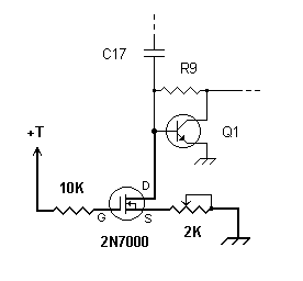
Next comes the 2N7000 FET. This is used to reduce the transmitter feed-through in the receiver by shunting the signal on the base of Q1 to ground. The amount of feed-through, and hence the sidetone level, is controlled by the 2K pot. When you are finished, the circuit will be as shown at the left (the three added components are shown in bold).
Prepare the 2N7000 as follows: With the flat side of the transistor facing you and the leads pointed down, bend the left-hand lead up beside the transistor body. Bend the center lead up in front (the flat side) of the transistor. You now need to carefully solder the remaining lead (the right-hand one, which is the drain lead) to the front pad of R9 (the pad that connects to C17 and Q1). Shape the lead so that a short section will just fit over the solder pad of R9. The bottom of the transistor should be about 3/16-in. above the board. The left-hand lead (the source lead) will be attached to the free lead of the 2K pot. After you have the two outside leads of the FET properly trimmed and bent into position, solder the drain lead to the front pad of R9 and the source lead to the lead from the pot. The gate (center) lead will be sticking up in front of the FET. Note: use a small soldering iron tip and relatively high temperature (750-800 degrees F) when soldering to the R9 pad and be quick! Hold the wire from the FET on the pad and touch the iron to the lead only long enough for solder to flow from the pad to the wire. After you have secured the FET in place by soldering the other lead to the pot, you can use a little solder if necessary to touch up the connection to the pad. Again, leave the iron on the pad only long enough to get the solder to flow. If you get too much solder on the pad, remove the excess using desoldering wick.
Next, locate the two feed-through holes between R19 and C27. The hole nearest R19 connects the "+T" line from the top to the bottom of the board; this is the one that you want. The 10K resistor connects between this hole and the gate (center lead) of the 2N7000. Bend one lead of the resistor at a right angle about 1/4-in. from the resistor body. Feed the bent end of the lead into the hole and trim the other lead so that it can be soldered to the gate lead of the FET. The resistor should be positioned about 3/16-in. above and parallel to the board. (If you did not remove the board from the case, trim the bent resistor lead so that it will not extend below the board and short to the case. Otherwise, you can trim the lead after it is soldered.) Solder the resistor in place and trim any lead excess.
Now solder the 2.2K resistor between the front of R28 and R29 (immediately to the left of C27). The pads to which you will solder the resistor are the ones that connect to Q8. The resistor should be positioned on top of R28 and R29 with the leads bent to touch the two solder pads. A 1/8W resistor works best for this, but a 1/4W one can also be used. Again, be careful not to heat the pads to long or be sloppy with solder.
When you have the 2.2K resistor in place and the leads trimmed, solder the 0.22µF capacitor between the front pad of R29 (the same one to which the 2.2K resistor is attached) and the lead of the 10K resistor that passes through the PC board.
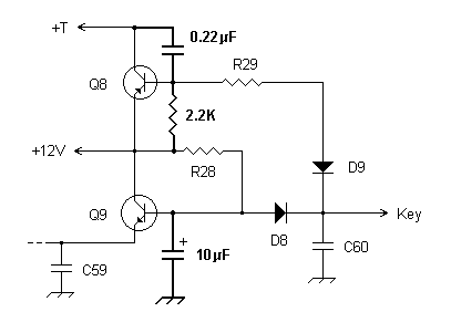
The 2.2K resistor and 0.22µF cap are used to shape the rise and fall time of the CW keying waveform. Without these components, the CW envelope risetime is very fast (about 0.1ms) resulting in minor but noticeable key-clicks. With these added components, the CW envelope rise and fall times will be about 2ms yielding very nice sounding keying. The new Q8-Q9 switching circuit will be as shown in the figure to the left (added components are shown in bold).
Now all that is left to do is solder the positive lead of the 10µF cap from the pad of D8 that connects to Q9 and R28 and the negative lead to ground. For the ground connection, use the feed-through hole between D5 and C60.
The 10µF cap ensures that the T/R switch (comprised of D4-D7) remains off a few milliseconds after transmitter output decays to zero so that no "thumps" or "clicks" will be heard in the sidetone. However, the receiver will still recover very quickly allowing full QSK operation.
The long recovery time of the receiver in its stock form was due to the AGC being blocked during transmit by a voltage applied to it through R30. However, if you just remove R30, the sidetone will be extremely loud and will still activate the AGC. The FET shunt from the base of Q1 to ground eliminates this problem.
Carefully check your work for solder splashes, connection errors, etc.
When you are satisfied that all is well, set the 2K pot to the middle of
its range, connect the rig to a power source, key, dummy load and
headphones. Apply power and key the rig; the sidetone should not have any
"clicks" or "thumps" and the receiver should recover almost
instantaneously on key-up. If not, then it’s time to retrace your steps!
If all is well, set the desired sidetone level with the audio pot set for
a comfortable level for receiving and enjoy true QSK operation!
————
Copyright © 2005, 2012 by Larry East, W1HUE ————
Page last updated on November 12, 2012