
Larry East, W1HUE
Tucson, Arizona
(contact author)
This article appeared in the June 1995 issue of the NorCal QRPp.
While giving my Ten-Tec Argonaut 509 a good going over recently, I discovered that the keyed output waveform is far from ideal; its fall time is very fast (less than 0.25ms) and its rise time ranges from greater than 5ms to less than 1ms depending on the setting of the output drive control. The fast fall time results in noticeable key-up clicks. Clicks can also occur on key-down when the drive control is set for maximum output. Since the keying circuit in my 509 is "stock" (at least it matches the schematic), I assume that these keying characteristics are fairly typical. I have not had access to other Argonaut models (505, 515) to check their keying waveform, but this condition may well be present in them also. If it is, the modifications described below may apply to the other models.
The keying signal for the 509 is derived from the "T" (transmit) control signal generated on the control board. "T" provides bias voltage for the RF amplifier and drivers, mutes the receiver and in conjunction with an "R" signal (basically the complement of "T") performs various other control functions necessary to switch from receive to transmit. The "T" signal is also fed to the CW drive control, R5, which is ganged with the microphone gain control, R7, and labeled as "DRIVE" on the front panel. A portion of "T", as determined by R7, is fed to the SSB generator board and is used to control the gain of the IF mixer when in CW mode. In CW mode, this mixer is purposely unbalanced in order to provide a carrier signal; controlling the mixer gain consequently controls the carrier level. In SSB mode, the mixer is balanced and runs at maximum gain; the SSB signal level is then set by R7 which controls the microphone amplifier gain. The rise time of the CW signal so generated is determined by a 0.22µF capacitor (C18) and R5; however, as the setting of R5 is changed, the rise time is changed as well. To make matters worse, a zener diode, D1, on the SSB generator board used to limit the gain controlling voltage to the mixer will cause the rise time to become very short if R5 is turned beyond the point at which output power no longer increases. (No additional output power is produced because the control voltage is being clamped by D1). When the key is released, the CW carrier decays with the "T" signal decay, which is very fast. Hence the presence of key-up clicks.
After I got all of this figured out, It became clear that the way to control the rise and fall times of the CW carrier was to control the rise and fall times of the "T" control signal itself. This can be done by a fairly simple modification to the control board. The modification consists of removing capacitor C18 and modifying the "Transmit" switching circuit to provide the necessary shaping. The modified switching circuit is shown in Figure 1. After this modification the keyed output rise time will be about 3ms independent of the drive control setting, provided it's not turned beyond the point of maximum output. The fall time will be about 2ms, slow enough to eliminate the generation of key-up clicks. (Increasing the fall time aggravates another problem which must also be fixed, as described below.)

Figure 1. Modified circuit to generate transmit control signal.
To make this modification, proceed as follows (I assume that you have a manual for the 509; use it to locate the components referred to below):
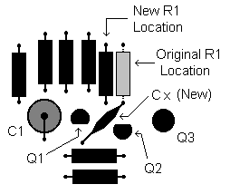
Figure 2. Parts placement on control board.
Sorry, but you're not finished yet! The "T" signal is used to disable RIT offsets during transmit (a small VFO offset is still present, but much less than during receive). The timing for disabling the RIT during transmit is rather marginal in an unmodified 509, but it seems to work OK until the "T" signal fall time is increased. Increasing the fall time of this signal results in the RIT offset (if any) being restored before the transmitter output is reduced completely to zero. This can produce noticeable "thumps" (not really "clicks") at the very end of every transmitted "dit" and "dah" when an RIT offset is in use; not a good situation. Fortunately the problem is easily solved by using the "R" signal for RIT disabling rather than "T". The "R" signal drops to zero shortly before "T" increases above zero, and begins rising with a long time constant when "T" returns to zero.
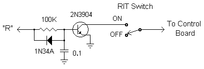
Figure 3. Inverter circuit required to use the "R" signal to
disable RIT during transmit.
A simple inverter, shown in Figure 3, is required in order to use the "R" signal to disable RIT offsets. I built this circuit on a small piece of "perf-board" and mounted it "spider web" style above the RIT control pot; the wire from the collector of the inverter transistor to the switch on the rear of the pot holds the board in place. The RC time constant at the base of the transistor insures that the RIT offset will remain disabled until the transmitter output is completely off. The diode across the base resistor discharges the capacitor quickly when the "R" signal drops to zero ensuring that the VFO frequency will be completely switched back from any RIT offset before the transmitter output begins rising. With the component values shown, the RIT is switched off about one millisecond before any measurable transmitter output and switched back on about one millisecond after transmitter output falls to zero.
To complete the keying modification, proceed as follows:
That's it; now its time to try it out! If you have an oscilloscope, use it to verify the keying waveform; otherwise, listen to the output on another receiver (being careful not to overload it). Also make sure that the RIT still works, and listen to the transmitter output while varying the RIT control (with it ON, of course!); there will be some shift in transmitter frequency, but there should be no "thumps" or other extraneous output resulting from varying the RIT control.
For best CW shaping at maximum power output, increase the drive control until the power output no longer increases and then back it off just a bit. Setting the drive control "wide open" will result in key clicks and not produce any additional output power. You should also keep in mind that running much more than 5W output from "stock" finals can degrade the spectral purity of the output signal.
Now you can operate you faithful little Argonaut without fear of
generating any interference from a poorly shaped CW signal!
————
Copyright © 2005, 2012 by Larry East, W1HUE ————
Page last updated on June 18, 2012